
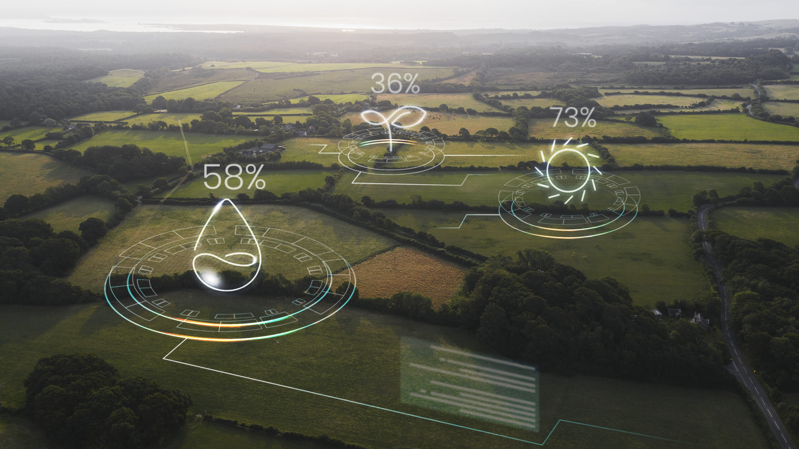
Agri IoT – Soil & Water Monitoring
Our Customer proposed a requirement of Handheld Device, Humidity, Soil & Water Sensors, Wireless Connectivity – Bluetooth
etc which were able to provide.
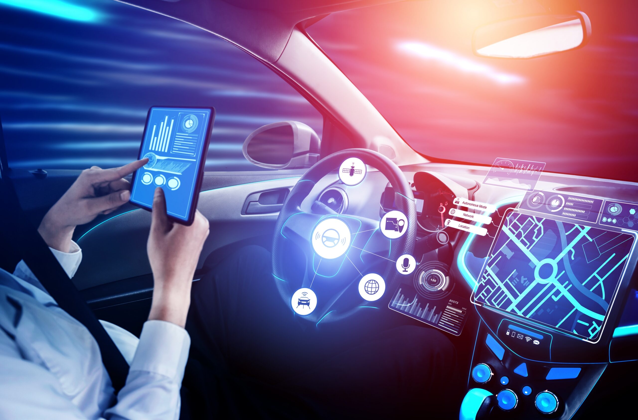
Automotive System
Our Customer had a challenge of Complex multiprocessor system for Autonomous Automotive application which we resolved.
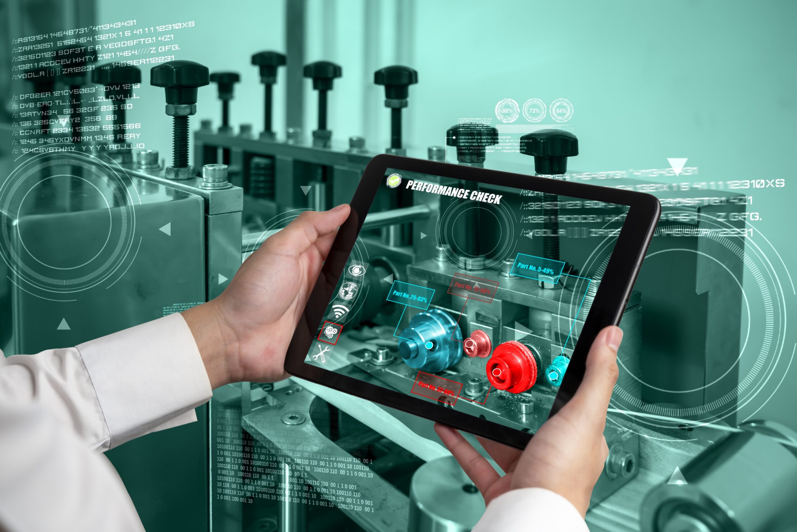
IIOT – Water Quality Monitoring
Our Customer required a Realtime data monitoring and control system with sensors, pumps and wireless connectivity in industrial environment.